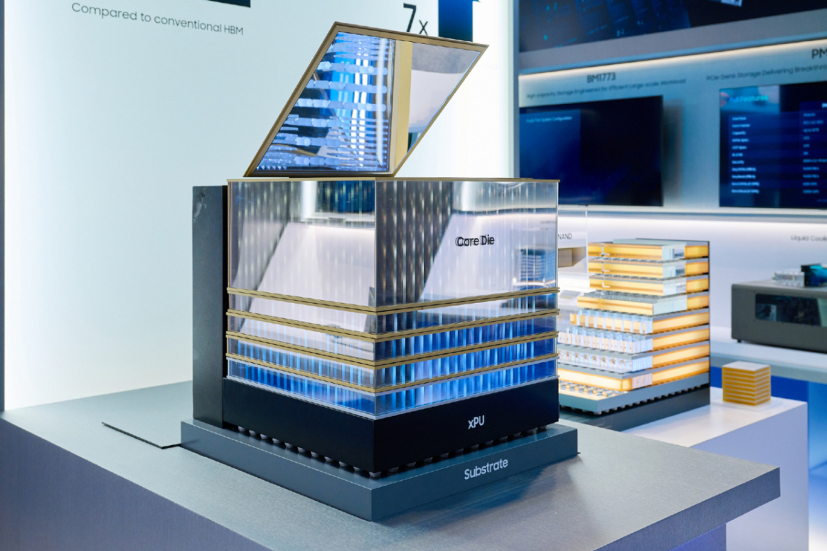
As of August 6, 2026, Samsung Electronics has unveiled the world's first 'zHBM' memory structure, which stacks memory directly on top of a processor. Debuted as a concept model at the FMS 2026 exhibition in the US, the design is expected to deliver far greater performance than today's 8th-generation HBM5 chips.
Key points
- Samsung unveiled the world's first zHBM concept — memory stacked directly atop a processor — at FMS 2026 in Santa Clara, California.
- zHBM is expected to deliver up to 4-8x the performance and more than 3x the power efficiency of HBM5, which hasn't reached mass production yet.
- At the same event, Samsung also debuted the world's first V10 BV NAND, stacked beyond 400 layers, plus zNAND-O, a NAND structure built for on-device AI.
- Samsung emphasized its unique ability to combine memory, logic chips, foundry and advanced packaging into one integrated AI semiconductor solution.
Samsung Electronics took the stage at FMS 2026 — the world's largest memory and storage trade show, held over three days in California — to unveil a concept model of its next-generation zHBM memory architecture, a world first. The show ran August 4-6, and Samsung filled its booth with more than 30 products spanning DRAM, NAND and storage, all displayed inside a booth designed to resemble an AI cloud server.
zHBM breaks from the traditional approach of placing memory chips beside a GPU or AI accelerator. Instead, it stacks memory directly on top of the processor. Samsung says the design should deliver 4x to 8x the performance and more than 3x the power efficiency of HBM5, the eighth-generation standard that hasn't reached mass production yet. Thermal resistance — a measure of how much heat builds up — is expected to drop by more than half, and Samsung said it can customize the interlayer between the memory and accelerator for individual customers, adjusting capacity and performance to spec.
At the same event, Samsung also debuted the V10 BV NAND, a new flash memory chip stacked beyond 400 layers — another world first. The chip combines a technique that manufactures cells and circuits separately before bonding them vertically, wafer bonding, and a three-way split manufacturing process, boosting memory density 58% over the prior generation. Samsung also introduced zNAND-O, a structure that stores only the frequently accessed portions of large AI model data on NAND flash, which the company says can cut memory build costs to roughly one-sixth of current levels without sacrificing performance.
In the show's keynote, a Samsung DRAM development executive noted that token volumes used in AI inference have jumped more than 100-fold over the past two years amid the spread of agentic AI, making memory a key bottleneck in AI systems. Samsung Executive Vice President Lee Jin-yeop said Samsung is the only company that spans memory, logic chips, foundry and advanced packaging, and that it plans to use that breadth to offer integrated solutions across the entire AI semiconductor stack.
FAQ
How is zHBM different from traditional HBM?
Traditional HBM sits beside the processor, but zHBM stacks vertically on top of it, shortening the distance data has to travel.
When will zHBM appear in actual products?
What Samsung showed is a concept model; a commercial launch timeline hasn't been set yet.
What is FMS 2026?
It's the world's largest trade show dedicated to memory and storage technology, held in Santa Clara, California.
More from Korea today
Seoul's 13th Tropical Night Amid Extreme Heat Alert →‘The Odyssey’ Sellout Fuels Premium Cinema Boom →
📎 원문 보기 · Sources


머니투데이 · Aug 06, 2026AI가속기 '위'에 HBM 쌓는다… 삼성, 차세대 3D 메모리 공개 - 머니투데이Read the full story & photos at the source →
Leave a Reply